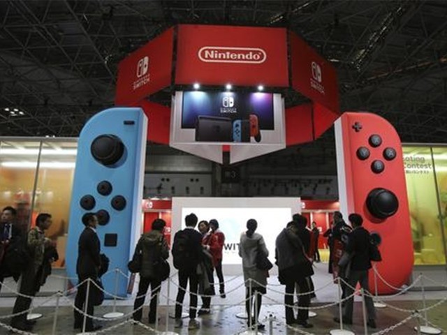
On May 20th, according to media reports from The Japan Times, the news that Samsung Electronics has obtained the chip manufacturing order for Nintendo Switch 2, although it shows prospects for cooperation from a technical perspective, from a deeper technological perspective, this decision reveals multiple technological compromises and future risks behind it. In the selection of processor design and manufacturing nodes, Nintendo and NVIDIA seem to pursue practical feasibility, but in fact, they also reflect problems such as hesitation in applying advanced processes, slow evolution of architectures, and insufficient utilization of computing power potential.
First of all, choosing Samsung's 8-nanometer process itself means a concession to advanced manufacturing processes. The current chip manufacturing industry has widely entered the 5nm and even 3nm era. Especially in the mobile and consumer electronics markets, Apple, AMD and Qualcomm have all adopted TSMC's 5nm and below processes on a large scale. Against this backdrop, Nintendo's new generation of consoles still adopts Samsung's 8nm process, which inevitably seems outdated. Although Samsung's 8nm process does not use extreme ultraviolet (EUV) technology, which to some extent reduces manufacturing costs, this "mature" node cannot mask its disadvantages compared to advanced processes in terms of energy efficiency ratio, transistor density and heat dissipation performance. Especially when game consoles need to balance high performance and portability, the use of the 8nm process will restrict the stability and energy efficiency of chips during long-term high-load operation.
What is more worthy of attention is that the ARM Cortex-A78C architecture adopted by the Tegra T239 chip itself is no longer the latest design. Although Cortex-A78C has improved compared to A77 or A76, when facing the currently widely used Cortex-X series and the new generation of ARMv9 architecture, its performance, instruction set expansion, and support for AI computing are all insufficient. Especially, the A78C is optimized for high-performance computing rather than extreme performance. Its architecture is more adapted to Chromebooks or lightweight laptops, and its performance in high-intensity graphics processing scenarios may not fully meet the demands of new-generation games.
The CPU section adopts a 6+2 core layout. Although it reflects the differentiated consideration of games and system tasks, it also highlights a structural simplification and conservatism. Unlike modern smartphone SoCs that widely adopt a three-tier heterogeneous design of "super-large core + large core + small core", the T239 still remains at the dual task division stage, which limits its flexibility in power consumption control and concurrent multi-task processing. This design may lead to insufficient performance release during the actual game operation, especially in the Dock mode. If the high-performance cores are not scheduled reasonably, the resource utilization rate will not be optimized.
Although the GPU is equipped with the Ampere architecture, featuring 1,536 CUDA cores and supporting DLSS 2.x/3.x technology, this is also a clear "architecture recycling" strategy. The Ampere architecture was the product generation of NVIDIA in 2020, which was used for the RTX 30 series desktop graphics cards at that time. Currently, the mainstream Gpus in the PC market have long entered the Ada Lovelace architecture cycle. Adapting the old architecture to the new host, although technically feasible, is essentially a reuse of the existing design rather than a brand-new GPU solution tailored for the host. Although this approach saves development costs, it also means that the overall GPU performance cannot compete with the current PC-level graphics processing capabilities. Furthermore, the 1,536 CUDA cores can theoretically achieve a peak computing power of 4.3 TFLOPs when the actual frequency is relatively low. However, this is merely an ideal state. In actual scenarios, due to power consumption and heat dissipation bottlenecks, it is difficult for them to operate stably at the highest frequency.
Regarding the frequency, it is only 561MHz in handheld mode, which clearly reflects the extremely restrained demand for power consumption. But this also directly affects the game's picture performance and frame rate stability. Although it supports dynamic frequency adjustment, with a maximum frequency of 1400MHz in host mode, the performance gap caused by switching modes poses a challenge to developers: it is necessary to adapt to two extreme performance intervals, making it difficult to uniformly optimize the experience. Furthermore, such a low frequency range will form a performance bottleneck for contemporary game rendering technologies, especially for computationally intensive features such as ray tracing and physical destruction simulation.
Although the memory has been upgraded to 12GB LPDDR5X, which seems to be an enhancement, from the perspective of technical utilization, allocating 9GB exclusively for gaming is not the best optimization solution. Modern SoCs typically adopt a Unified Memory Architecture (UMA) to dynamically allocate memory resources between the system and the GPU. A rigid division between the system and the game memory may lead to insufficient processing of system tasks or redundancy of game memory, limiting the flexible scheduling ability of resources and being unfavorable for the future expansion of the complexity of the game system.
In terms of process technology selection, Nintendo abandoned TSMC's 7nm/8nm and turned to Samsung's 8nm. Although there were considerations of cost and yield, this was not without cost. Although Samsung's 8nm process does not use EUV and has a cost advantage in the initial production, it still lags behind TSMC's N7 in terms of transistor density, leakage control and process consistency. From the experience of the Samsung 8nm products that have been launched on the market (such as the RTX 30 series), their high power consumption and heat generation problems have always been criticized by users. This may also extend to the battery life and noise performance of the Switch 2, especially in the handheld form. The heat dissipation space is limited, and the thermal design power (TDP) of the chip and surface temperature control will become technical challenges.
As for the claim that "performance upgrades will be carried out using the 5nm process in the future", it seems more like a packaging of a market launch strategy. In the current environment where the chip cycle is getting longer and longer, designing two generations of host SoCs and relying on different nodes for manufacturing not only increases the cost of software adaptation but may also lead to user differentiation. If future versions switch to the 5nm process while early players are restricted to the 8nm version, it will create a technological gap and force game developers to adapt to both performance standards simultaneously, thereby leading to platform fragmentation.
Overall, this technological collaboration between Nintendo and NVIDIA as well as Samsung more reflects a recycling and assembly of existing architectures and processes rather than a comprehensive technological upgrade for the future. From process selection, chip architecture to memory scheduling and GPU specifications, although the overall solution meets functional requirements, it lacks innovation and technological leadership, revealing Nintendo's conservative thinking in the pace of hardware updates and also NVIDIA's tendency to reuse resources in its custom chip strategy. In the future, if confronted with high-performance games and more complex graphics processing tasks, this combination of technologies may soon show signs of fatigue.

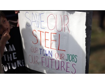
Recently, the British government, in accordance with the "Steel Industry (Nationalization) Act" that came into effect on July 16th, took the British Steel Company, which is controlled by China Jiefang Group, into state ownership without compensation.
Recently, the British government, in accordance with the "S…

On July 23rd local time, the US Trade Representative Office…

The international crude oil market saw a sharp one-sided ri…
Recently, the geopolitical confrontation between the United…

The New York Times has recently clashed with the Trump admi…

Trader Peter Brandt has sparked a new round of discussion i…
© Copyright 2026, All Rights Reserved