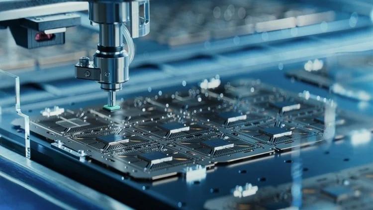
Vertical stacking of semiconductor chips in 3D integrated circuits to improve performance, reduce space occupation, and enhance energy efficiency. This technology achieves higher density, faster data transmission, and lower power consumption by integrating multiple layers of circuits into a single package. The main advantages include compact design, faster speed, and cost-effectiveness. 3D ICs are used for advanced applications such as high-performance computing, consumer electronics, and automotive systems due to the demand for more powerful and efficient electronic devices.
Firstly, the 3D integrated circuit market is expected to be worth $16.1 billion in 2024 and is projected to reach $59.4 billion by 2030, with a compound annual growth rate of 20.5% during the 2024-2032 forecast period. The driving force for growth comes from the advancement of semiconductor technology and the increasingly widespread applications in the fields of consumer electronics, telecommunications, and automobiles. The semiconductor industry has undergone a transformation, with new manufacturing methods greatly improving the performance of chips. A concept that is receiving increasing attention is the three-dimensional stacking of device layers, which is becoming increasingly important due to challenges in device miniaturization.
Secondly, a specific technology called single-chip 3D integration has become popular. It involves the formation of upper layer, active semiconductor layer, and lower layer materials. Compared with traditional 3D stacking technology, this method can achieve faster interlayer electron movement speed and higher interlayer connection density, thereby improving semiconductor performance. In M3D integration, the lower layer devices can be fabricated using traditional front-end and back-end processes, but the upper layer devices should use materials compatible with the lower layer to avoid defects or strains in the lower layer devices. In modern semiconductor manufacturing, people are constantly researching how to improve multi-layer interconnect technology that connects different metal layers. Only with the interconnection of conductive layers can 3D integrated circuits operate effectively. Researchers have developed an innovative multi-layer metal interconnect scheme that involves solvent-free patterned insulation layers to create interconnect regions, ensuring reliable electrical connections between different layers of metal.
On the other hand, using this technology, the team successfully manufactured the highest stacked organic transistor in a solvent-free manner, a three-dimensional organic integrated circuit consisting of five transistors and 20 metal layers. These transistors exhibit excellent characteristics, including a high on/off current ratio of approximately 107, no hysteresis behavior, and excellent device to device consistency.
In addition, the semiconductor industry is constantly innovating to meet the demand for higher performance, larger storage capacity, and higher energy efficiency. Among these advancements, 3D NAND technology stands out as a transformative development in the field of memory storage. 3D NAND and other emerging trends are expected to shape the future of semiconductor manufacturing. According to analysis, the market size of 3D semiconductor packaging is expected to increase from $9.43 billion in 2022 to over $35.3 billion in 2031, with an estimated growth of $10.73 billion by 2023 and a compound annual growth rate of 16.1% from 2023 to 2031.
3D XPoint, jointly developed by Intel and Micron, represents a new type of non-volatile memory that bridges the performance gap between DRAM and NAND flash memory. Compared to traditional NAND, this technology provides faster data access speed and higher durability, making it suitable for various high-performance applications. Compared to NAND flash memory, 3D XPoint has significantly faster read and write speeds, in some cases even up to 1000 times faster, making it an ideal choice for real-time data processing applications and high-performance computing tasks.
Overall, the future of semiconductor manufacturing is marked by breakthrough innovations such as 3D NAND, advanced lithography technology, heterogeneous integration, and emerging computing paradigms such as quantum and neural morphology computing. These advancements are expected to bring higher performance, higher efficiency, and new features, driving the next wave of technological progress in various industries. As these technologies mature, they will redefine the landscape of semiconductor manufacturing, paving the way for future innovations that will continue to push the boundaries of possibilities.

Driven by the Trump administration's push to relax financial regulations and the recovery of investment banking business, the market value of the six major banks in the United States has cumulatively increased by approximately 600 billion US dollars by 2025.
Driven by the Trump administration's push to relax financia…
On Christmas evening, U.S. President Trump posted on social…
According to multiple foreign media reports, the recent fin…
The middle class, once regarded as the cornerstone of Ameri…
On December 19th local time, the US military launched a lar…
The Boxing Day sunshine should have cast a false glow of pr…