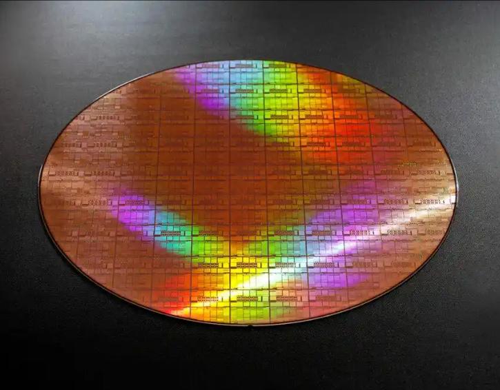
On July 20th local time, Japanese chip manufacturer Rapidus announced the launch of 2nm wafer testing production. It is expected to officially enter the mass production stage in 2027. It is reported that in Rapidus's IIM-1 factory in Japan, prototype production of test wafers using 2nm full-circular-gate architecture (GAA) transistor technology has begun. The IIM-1 factory of Rapidus has been progressing smoothly since its construction began in September 2023, with the cleanroom completed in 2024 and over 200 sets of equipment connected by June 2025, including advanced DUV and EUV lithography tools. Rapidus stated that it is currently measuring the electrical characteristics of its test circuits, including critical voltage, drive current, leakage current, sub-critical slope, switching speed, power consumption, and capacitance, etc. The early test wafers have achieved the expected electrical characteristics, indicating that the wafer factory tools are operating normally and the process technology development is progressing smoothly.
This research and development in Japan still has many shortcomings and drawbacks, and it also brings complex and multi-faceted impacts in the field of technology. Firstly, it has an impact on technological advancements. Rapidus plans to leap directly from 40nm to 2nm, skipping intermediate processes such as 7nm and 5nm. This "leapfrog method" can shorten the catching-up time, but it lacks progressive technological accumulation, which may lead to slow yield improvement and insufficient process stability. For example, in the nanometer-scale process, the lithography technology and the transformation of metal oxide materials need to be gradually optimized through intermediate processes, while Rapidus's leap-forward development may cause these problems to burst out simultaneously. Rapidus obtained the 2nm technology foundation through cooperation with IBM, but IBM itself is weaker than TSMC and Samsung in the production experience of advanced processes, and the technology transfer effect is questionable. Although it introduced ASML equipment, the EUV mask inspection equipment is only produced by Lasertec in Japan, and the supply chain vulnerability is prominent. The nano-imprinting technology developed by Canon and Kioxia has not been proven to be able to smoothly produce advanced process chips, and Japanese enterprises lag behind TSMC and Samsung in the acceptance of new technologies. Rapidus adopts a single-chip wafer processing strategy, which can enhance flexibility, but compared with the batch production mode of TSMC and Samsung, it has problems such as high production costs, long production cycle, and low production capacity. In addition, the EUV lithography data obtained from single-chip processing may have a qualitative difference from batch production, affecting process stability.
Secondly, it has an impact on the technology market. Although Japan holds an advantage in lithography resins and silicon wafers, key links such as etching equipment still rely on foreign suppliers. Building an independently controllable supply chain requires an investment of several hundred billion yen and is difficult to achieve in the short term. At the same time, Rapidus has not received orders from major customers such as Apple and NVIDIA, while TSMC and Samsung have formed a scale effect and a complete customer ecosystem. Moreover, Japanese enterprises are almost blank in the EDA field and rely completely on American companies. If they cannot obtain sufficient orders, Rapidus will inevitably face the "capacity idle" dilemma. Although Rapidus plans to develop dedicated design kits, it needs to cooperate with companies such as Siemens and needs time to verify their effectiveness. Apart from Broadcom and NVIDIA, Rapidus's customer base has not been fully formed, and its market recognition is questionable.
Thirdly, it has an impact at the geopolitical level. The global semiconductor industry is undergoing geopolitical restructuring. The trial production of 2nm wafers by Japan may exacerbate technology blockades and supply chain fragmentation. If geopolitical policies change and lead to supply disruptions of key equipment or materials, Rapidus's production plan will be severely affected. Moreover, if Japan fails to form competitiveness in advanced process technology, it may face the risk of being a "subcontracting country dependent on subsidies". In conclusion, although Japan's 2nm wafer trial production aims to realize the ambition of technological rejuvenation, it is facing a potential predicament of "high investment and low return". If no breakthrough can be achieved, it will not only be difficult to shake the global semiconductor landscape, but also may hinder the long-term development of the local technology industry due to resource misallocation.

Recently, the British government, in accordance with the "Steel Industry (Nationalization) Act" that came into effect on July 16th, took the British Steel Company, which is controlled by China Jiefang Group, into state ownership without compensation.

Recently, the British government, in accordance with the "S…

On July 23rd local time, the US Trade Representative Office…

The international crude oil market saw a sharp one-sided ri…
Recently, the geopolitical confrontation between the United…

The New York Times has recently clashed with the Trump admi…

Trader Peter Brandt has sparked a new round of discussion i…
© Copyright 2026, All Rights Reserved