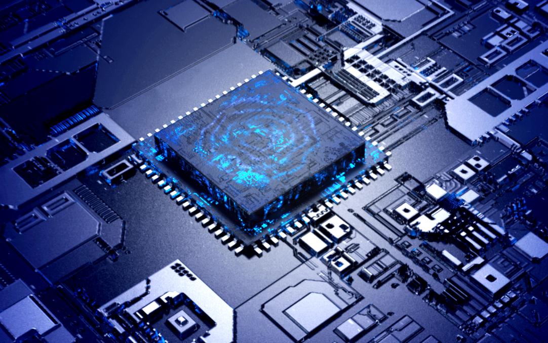
Recently, Google reached an agreement with London cloud service provider Fluidstack to deploy its self-developed AI chip TPU in third-party data centers for the first time, marking Google's official break from the closed strategy of "only self built data centers" and launching a comprehensive attack on the AI chip market led by Nvidia. This competition, driven by technological iteration, ecological expansion, and capital game, is reshaping the global AI computing power landscape.
The competitiveness of Google TPU lies in its continuous technological iteration. The sixth generation Trillium TPU has achieved a peak computing power of 42.5 exaflops, increased high bandwidth memory capacity by three times compared to the previous generation, and optimized cost efficiency by 40%. The upcoming seventh generation Ironwood TPU focuses more on AI inference scenarios, and its low latency architecture can support real-time interactive applications, filling the market gap. Behind technological breakthroughs lies the improvement of the ecosystem. Google has solved the key obstacle of external deployment of TPU - programming compatibility - through optimization of the JAX framework. By 2025, the support efficiency for TPU by JAX will increase by 60%, and developers can seamlessly migrate PyTorch models to TPU clusters directly. This full stack optimization of "hardware software development tools" enables TPU to improve training efficiency by 25% compared to Nvidia H100 and reduce inference costs by 35%.
Google's strategic transformation is reflected in three dimensions: breaking through customer base, leveraging capital, and cultivating a developer ecosystem. Through third-party cloud service providers such as Fluidstack, TPU has entered Nvidia's core customer base for the first time. Fluidstack provides computing power leasing for AI startups such as Mistral. By adopting TPU in its New York data center, customers can save 40% on model training costs. Google provides Fluidstack with a $3.2 billion "backstop" financing to ensure that its data center construction is not restricted by funding. This "chip+capital" bundling model is replicating the ecological barriers built by Nvidia through investments in companies such as CoreWeave. From February to August 2025, the activity of TPU related developers on Google Cloud will increase by 96%, and companies such as Anthropic and xAI will start recruiting TPU core engineers. The display technology community is migrating to TPU.
Nvidia's response strategy highlights its anxiety, mainly reflected in three aspects: technology, ecology, and market. On a technical level, Nvidia emphasizes the versatility advantage of GPUs, but faces challenges from TPU specific architectures. For example, in Llama 3 model training, the cluster scaling efficiency of TPU is 18% higher than that of A100 GPU. At the ecological level, Nvidia locks in customers through the CUDA ecosystem, but Google retaliates with "open source framework+low cost". The MIT license for JAX allows developers to freely modify, while Nvidia's CUDA toolkit requires paid licensing. At the market level, Nvidia prioritizes supplying Blackwell chips to allies such as CoreWeave, but Google breaks the supply monopoly through new channels such as Fluidstack. It is estimated that the external deployment of TPU can increase Google's market share in AI chips from 12% to 25%.
From a capital perspective, D.A. Davidson analysts point out that if the TPU business is merged and spun off from DeepMind, the valuation could reach $900 billion. This judgment is based on three pivot points: technological scarcity, customer stickiness, and ecological closure. TPU is the world's only mass-produced 10 trillion yuan secondary AI chip, with a computing power density 1.8 times that of NVIDIA DGX H200. Google Cloud customers such as Apple and Midjourney have formed a habit of using TPU, and the migration cost is high. Combining DeepMind's AI algorithm advantages, TPU can build a vertically integrated system of "chip model application", similar to Apple's M-series chip ecosystem.
Google's attack is driving three major changes in the AI chip industry: downward pressure on prices, differentiation of technology routes, and restructuring of geopolitical computing power. The low-cost strategy of TPU has forced Nvidia to lower the price of H200 chips by 15%, giving small and medium-sized cloud service providers bargaining space. AI chips have shifted from a single path of "general-purpose GPU" to a dual track system of "dedicated ASIC+general-purpose GPU". AMD、 Intel and other companies are accelerating the development of competitors such as MI300X and Gaudi 3. Google plans to deploy TPU regional centers in Saudi Arabia, Singapore, and other places to weaken Nvidia's monopoly on North American computing power clusters.
The competition between Google and Nvidia is essentially a battle between the "closed ecosystem" and "open alliance" models. When TPUs begin to appear in the data centers of Nvidia's core customers, when the JAX framework becomes a new favorite among developers, and when a valuation of $900 billion is no longer a fantasy, the AI chip market is ushering in a true "Darwin moment" - only continuous innovators can survive in this computing revolution.

Recently, the British government, in accordance with the "Steel Industry (Nationalization) Act" that came into effect on July 16th, took the British Steel Company, which is controlled by China Jiefang Group, into state ownership without compensation.

Recently, the British government, in accordance with the "S…

On July 23rd local time, the US Trade Representative Office…

The international crude oil market saw a sharp one-sided ri…
Recently, the geopolitical confrontation between the United…

The New York Times has recently clashed with the Trump admi…

Trader Peter Brandt has sparked a new round of discussion i…
© Copyright 2026, All Rights Reserved