The South Korean government has announced its largest-ever industrial investment plan. Over the next 10 years, it will focus on semiconductor, artificial intelligence (AI) data centers and physical AI technologies, aiming to drive over 200 trillion won of corporate investment. This will help build South Korea's AI ecosystem, promoting balanced national development and strengthening the country's technological edge during the global industrial restructuring.
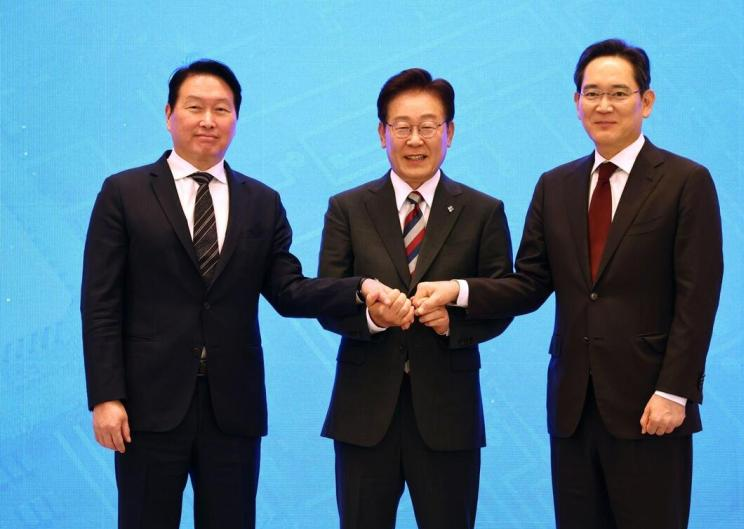
On Monday (June 29th), South Korean President Lee Jae-myung attended a live TV press conference along with Samsung Electronics Chairman Lee Jae-yong and SK Group Chairman Choi Tae-yon. He said that South Korea must grasp the core elements of AI more quickly than other countries. Semiconductors, physical AI, and AI data centers will be the three main pillars driving South Korea to achieve a new round of leapfrog development.
Lee Jae-myung emphasized that in the AI era, major countries such as the United States and China are engaged in intense competition for industrial dominance. Korea must, through the collaboration between the government and enterprises, accelerate the establishment of a Korean-style AI ecosystem.
In the semiconductor industry, South Korea plans to transform the relatively underdeveloped Hwangsan area in the southwest into the second-largest semiconductor production base after the capital region. According to the plan, enterprises will invest approximately 800 trillion won in the southwest region to build four new wafer factories, and simultaneously cultivate supporting enterprises and a talent ecosystem.
At the same time, the construction of the semiconductor base in the capital region will accelerate. The completion time of the last wafer factory in the Yongmun National Industrial Park and the ordinary industrial park will be seven years and 12 years earlier than the original plan respectively. The goal is to expand the storage chip production capacity to twice the current level within the next five years.
Samsung Electronics' CEO Lee Jae-yong said on the same day that Samsung is considering making Gwangju a candidate site for its next-generation semiconductor park, as the area has advantages in terms of electricity, water supply, human resources and infrastructure. This is also the first time that Samsung has publicly disclosed that it may build a large-scale semiconductor production base outside the capital region.
According to the plan, the Chungcheong region will be developed into an advanced packaging center, with a total investment of approximately 81 trillion won. Located in the central part of South Korea, the Chungcheong region is a key transportation hub and an emerging hub for technology industries. The government plans to support the expansion of high-bandwidth memory (HBM) production in places such as Wonyang and Cheonan in South Chungcheong Province, and to promote the early implementation of the HBM packaging project in Cheongju.
To seize the markets for next-generation memory, edge AI semiconductors and defense semiconductors, South Korea plans to invest at least 30 trillion won over the next 15 years for the entire cycle of research and development, design, verification and manufacturing.
In terms of AI infrastructure, the government will collaborate with major enterprises such as SK, GS and Naver to build an AI data center with a total capacity of 8.4 gigawatts, with an investment of approximately 550 trillion won. South Korea hopes to add another 10 gigawatts of data center facilities by 2035, increasing the national total capacity to 18.4 gigawatts and accumulating an investment of over 1 trillion won.
As for the development of physical AI, the South Korean government plans to build a mass production system for humanoid robots centered in Sinmun-gu area, and promote the transformation of automotive and household appliance component enterprises in Daegu and North Gyeongsang Province to become suppliers of robot components.
Lee Jae-myung said that the presidential office will appoint dedicated managers for the three major projects, and the president will personally supervise the implementation of these tasks. He emphasized that these three projects will determine the country's competitiveness in the next 20 to 30 years, and the government will fully accelerate the implementation of the related plans.
However, the feasibility of this grand plan has been questioned.
Experts point out that although spreading semiconductor investment to areas outside the capital region can help alleviate existing infrastructure bottlenecks, the construction of advanced wafer factories requires vast amounts of electricity and water resources, a mature supply chain, and highly skilled personnel. And new areas may not be able to meet these requirements in a short period of time.
The opposition party criticized that the government's promotion of large-scale industrial layout carried a strong "authoritarian economic" flavor.
The representative of the largest national force party in the parliament, Jeong Dongsik, said that when competing enterprises such as Samsung and SK simultaneously announced their investment plans at the same event, it reflected that the government had actually influenced the investment directions of these enterprises.
Former congressman Liu Cheng-myung also emphasized that enterprises should make investment decisions based on market logic, and the government should not overly interfere in corporate decisions.
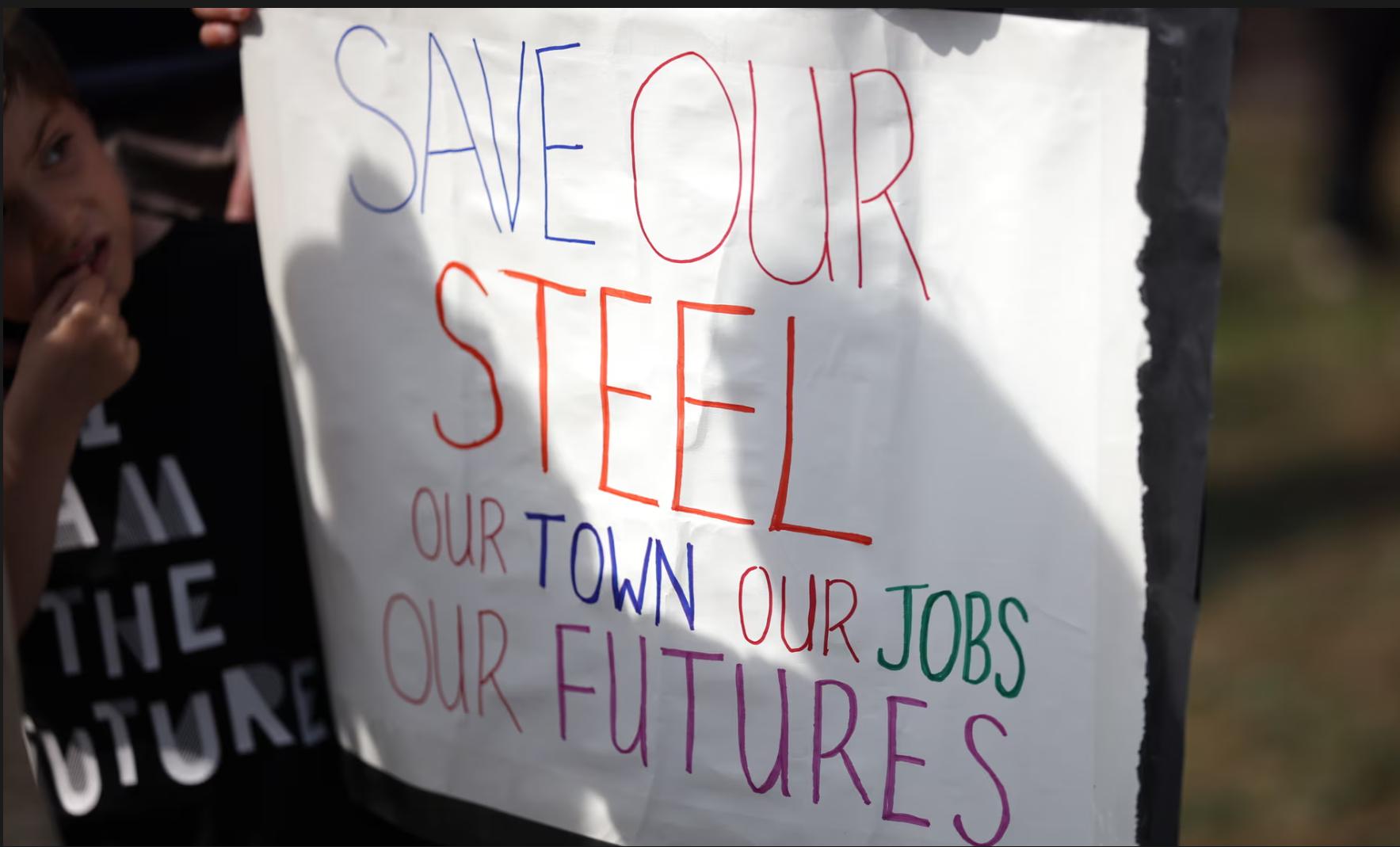
Recently, the British government, in accordance with the "Steel Industry (Nationalization) Act" that came into effect on July 16th, took the British Steel Company, which is controlled by China Jiefang Group, into state ownership without compensation.
Recently, the British government, in accordance with the "S…

On July 23rd local time, the US Trade Representative Office…

The international crude oil market saw a sharp one-sided ri…
Recently, the geopolitical confrontation between the United…
The New York Times has recently clashed with the Trump admi…

Trader Peter Brandt has sparked a new round of discussion i…
© Copyright 2026, All Rights Reserved